
Concept explainers
Videos
(a)
The value of the voltage
(a)
Answer to Problem 16.8P
The maximum value of the voltage
Explanation of Solution
Calculation:
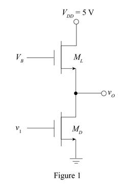
The given diagram is shown in Figure 1.
The expression for the voltage
Substitute
The expression for the enhancement mode NMOS inverter equation is given by,
Substitute
Conclusion:
Therefore, the maximum value of the voltage
(b)
The value of the voltage
(b)
Answer to Problem 16.8P
The maximum value of the voltage
Explanation of Solution
Calculation:
The expression for the voltage
Substitute
Consider the input voltage
The expression for the enhancement mode NMOS inverter equation is given by,
Substitute
Conclusion:
Therefore, the maximum value of the voltage
(c)
The value of the voltage
(c)
Answer to Problem 16.8P
The maximum value of the voltage
Explanation of Solution
Calculation:
The expression for the voltage
Substitute
Consider the input voltage
The expression for the enhancement mode NMOS inverter equation is given by,
Substitute
Conclusion:
Therefore, the maximum value of the voltage
(d)
The value of the voltage
(d)
Answer to Problem 16.8P
The maximum value of the voltage
Explanation of Solution
Calculation:
The expression for the voltage
Substitute
Consider the input voltage
The expression for the enhancement mode NMOS inverter equation is given by,
Substitute
Conclusion:
Therefore, the maximum value of the voltage
Want to see more full solutions like this?
Chapter 16 Solutions
Microelectronics: Circuit Analysis and Design


- Redesign the resistive load inverter for operation at a power level of 0.30 mW withVDD = 3.3 V. Assume VT O = 0.7 V. Keep theother design parameters the same. What is the newsize of MS and the value of R? (b) What are thevalues for NMH and NML ?arrow_forwardWhat is the power-delay product for a symmetrical CMOSinverter with (W/L)N = 2/1, (W/L)P = 5/1,VDD = 2.5 V, and C = 0.3 pF? (b) Repeat forVDD = 2.0 V. (c) Repeat for VDD = 1.8 V.? How much power does the inverter dissipate if it is switching at a frequency of 100 MHz?arrow_forwardFor an inverter with VIL = 0.46 V, VIH = 0.77 V, VOL= 0.08 V, and VOH = 1.2 V, find out the maximum value for the noise voltage in presence of which the inverter can work properly. Ans: 0.38 V.arrow_forward
- Problem 3 Consider a CMOS static inverter. Please be careful with units. The NMOS transistor has the following characteristics. The channel length is 350 nanometers. For NMOS: tox=10nm, Vm=0.25V, un=560cm²/vsec, W=700nm, L=350nm For PMOS: tox=10nm, Vtp=-0.35V, up=240cm²/vsec, W=700nm, L=350nm Compute the resistance R₁ for NMOS if the power supply voltage (Vad) is 1.25 volts.arrow_forwardAssume Vth = 1V and k = 50mA/V2. Given the schematic below, do the following: 1) Indicate and verify the state of each MOSFET and ?0 for the following input combinations. Fill-out the table below for each assumed state of the MOSFET for every input combination. Use ?ds,on approximation for linear operation. 2) Determine what kind of logic circuit is implemented in the circuit.arrow_forward2. Half-bridge inverter is supplied by voltage 400V and is controlled by sinusoidal PWM with modulation index 0.8. What is the value of amplitude of the fundamental component of the AC output voltage? of 1arrow_forward
- Question-3: Sketch the voltage transfer characteristic of the NMOS inverter circuit given in Figure 3 by calculating the output voltage Vour for Vin= 0, 2, 4, and 5 V. Find also noise margins. (K=1 mA/V2, V₁=1 V for the NMOS transistor.) Vin VDD=5V 5k Figure 3: NMOS inverter -Vout 21/2arrow_forwardDesign an asymmetrical inverter to meet the delay specificationa symmetrical CMOS reference inverter to provide a delay of 1 ns when driving a 10-pF load.(a) Assume VDD =2.5 V. (b) Assume VDD =1.8 V and VT N =−VT P =0.45 V. with (W/L)P = 2(W/L)N .arrow_forwardWhat will be the fundamental frequency for the following circuit if each inverter delay is 100 nsec? Outputarrow_forward
- In the single-phase, full-bridge inverter controlled by the single PWM control, the frequency of the reference signal determines:arrow_forwardA full-bridge inverter has a switching sequence that produces a square wave voltage across a series RL load. The switching frequency is 60 Hz, Vdc=100 V, R equals to 10 Ohm, and L equals 25 mH. The average current in the dc source is. Select one: O a. 52 A O b. None of the above O c. 4.41 A O d. 300 Aarrow_forwardAn inverter with a resistive load, VDD = 3.3 V, P = 0.1 mW, VL = 0.2 V, K'n = 60 UA/V2 and VT N = 0.75 V. The value of (W/L)S is:arrow_forward
 Introductory Circuit Analysis (13th Edition)Electrical EngineeringISBN:9780133923605Author:Robert L. BoylestadPublisher:PEARSON
 Delmar's Standard Textbook Of ElectricityElectrical EngineeringISBN:9781337900348Author:Stephen L. HermanPublisher:Cengage Learning
 Programmable Logic ControllersElectrical EngineeringISBN:9780073373843Author:Frank D. PetruzellaPublisher:McGraw-Hill Education
 Fundamentals of Electric CircuitsElectrical EngineeringISBN:9780078028229Author:Charles K Alexander, Matthew SadikuPublisher:McGraw-Hill Education
 Electric Circuits. (11th Edition)Electrical EngineeringISBN:9780134746968Author:James W. Nilsson, Susan RiedelPublisher:PEARSON
 Engineering ElectromagneticsElectrical EngineeringISBN:9780078028151Author:Hayt, William H. (william Hart), Jr, BUCK, John A.Publisher:Mcgraw-hill Education,